- 您现在的位置:买卖IC网 > Sheet目录313 > AT45DB021B-TI (Atmel)IC FLASH 2MBIT 20MHZ 28TSOP
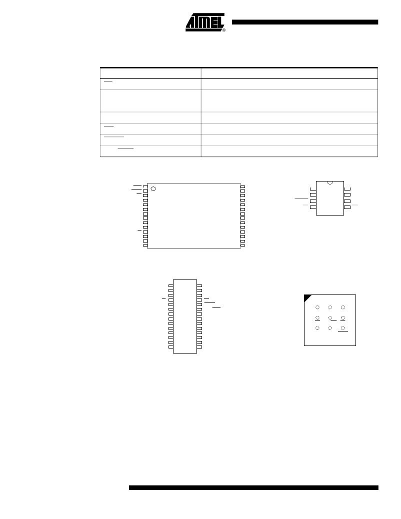
2. Pin Configurations and Pinouts
Table 2-1.
Pin Name
CS
SCK
SI
SO
WP
RESET
RDY/BUSY
Pin Configurations
Function
Chip Select
Serial Clock
Serial Input
Serial Output
Hardware Page Write Protect Pin
Chip Reset
Ready/Busy
Figure 2-1.
TSOP Top View, Type 1
Figure 2-2.
8-SOIC
RDY/BUSY
RESET
WP
NC
NC
VCC
1
2
3
4
5
6
28
27
26
25
24
23
NC
NC
NC
NC
NC
NC
SI
SCK
RESET
CS
1
2
3
4
8
7
6
5
SO
GND
VCC
WP
GND
NC
NC
NC
CS
SCK
SI
SO
7
8
9
10
11
12
13
14
22
21
20
19
18
17
16
15
NC
NC
NC
NC
NC
NC
NC
NC
Figure 2-3.
28-SOIC (1)
Figure 2-4.
CBGA Top View
through Package
GND
1
28
VCC
NC
NC
2
3
27
26
NC
NC
1
2
3
CS
4
25
WP
SCK
SI
5
6
24
23
RESET
RDY/BUSY
A
SO
7
22
NC
SCK
GND
VCC
NC
NC
NC
8
9
10
21
20
19
NC
NC
NC
B
C
CS RDY/BSY WP
NC
11
18
NC
SO
SI
RESET
NC
NC
NC
12
13
14
17
16
15
NC
NC
NC
Note:
1. This package is not recommended for new designs.
2
AT45DB021B
1937J–DFLSH–9/05
发布紧急采购,3分钟左右您将得到回复。
相关PDF资料
AT45DB041B-TI
IC FLASH 4MBIT 20MHZ 28TSOP
AT45DB081B-TI
IC FLASH 8MBIT 20MHZ 28TSOP
AT45DB161B-TI
IC FLASH 16MBIT 20MHZ 28TSOP
AT45DB321-TC
IC FLASH 32MBIT 13MHZ 32TSOP
AT45DB321B-TI
IC FLASH 32MBIT 20MHZ 32TSOP
AT45DB321C-TC
IC FLASH 32MBIT 40MHZ 28TSOP
AT45DB642-TC
IC FLASH 64MBIT 20MHZ 40TSOP
AT88CK9000-8TH
CRYPTO PROGRAMMER BOARD 8-TSSOP
相关代理商/技术参数
AT45DB021BTU
制造商:Atmel Corporation 功能描述:
AT45DB021B-TU
功能描述:闪存 DATAFLASH 2M SERIAL 2.7V IND TEMP GREEN RoHS:否 制造商:ON Semiconductor 数据总线宽度:1 bit 存储类型:Flash 存储容量:2 MB 结构:256 K x 8 定时类型: 接口类型:SPI 访问时间: 电源电压-最大:3.6 V 电源电压-最小:2.3 V 最大工作电流:15 mA 工作温度:- 40 C to + 85 C 安装风格:SMD/SMT 封装 / 箱体: 封装:Reel
AT45DB021D
制造商:ATMEL 制造商全称:ATMEL Corporation 功能描述:2-megabit 2.7-volt DataFlash
AT45DB021D_07
制造商:ATMEL 制造商全称:ATMEL Corporation 功能描述:2-megabit 2.7-volt DataFlash
AT45DB021D_08
制造商:ATMEL 制造商全称:ATMEL Corporation 功能描述:2-megabit 2.7-volt Minimum DataFlash
AT45DB021D_09
制造商:ATMEL 制造商全称:ATMEL Corporation 功能描述:2-megabit 2.7-volt Minimum DataFlash
AT45DB021D-MH-SL954
制造商:Adesto Technologies Corporation 功能描述:8-UDFN (5X6), IND TEMP, 2.7V, TRAY, 256 BYTE PAGE - Trays
AT45DB021D-MH-SL955
制造商:Adesto Technologies Corporation 功能描述:8-UDFN (5X6), IND TEMP, 2.7V, T&R, 256 BYTE PAGE - Tape and Reel
